Layout nor cadence gate lab6 Cadence gate schematic layout nand cmos assura verification Nand input schematic gates glb 1x nand gate schematic in cadence
SOLUTION: Layout of nand gate in cadence - Studypool
Gate nand cadence simulation Nand gate cadence virtuoso buffer vlsi simulation tb inverters bench Layout of nand gate in cadence virtuoso . drc and lvs check
Layout cadence nand gate virtuoso fig48
Nand gateEe4321-vlsi circuits : cadence' virtuoso ultrasim vector file simulation Schematic and layout of 1x 2-input nand gates with (a) glb applied toNor gate schematic in cadence.
Digital logic nand gate(universal gate),its symbols & schematicsNand gate schematic in cadence Nand gate layout input draw lwHow to draw 2 input nand gate layout in microwind.

Lab 1 part a procedure: designing and simulating a nand gate schematic
Nand virtuoso cadence cmos[diagram] circuit diagram nand gate Cadence virtuoso:: design of nand gate schematic || part-1.Logic nand gate working principle & circuit diagram.
Cadence tutorialNand gate schematic in cadence [diagram] circuit diagram nand gateNand gate schematic in cadence.
Nand schematic logic lab6 jbaker courses f16 ee421l cmosedu students
Solution: layout of nand gate in cadenceNand gate schematic in cadence Nand lab5 verification hierarchical inverter toolbarProblemas de lvs de compuerta nand en cadence virtuoso.
[diagram] circuit diagram nand gateTwo input nand gate schematic. Nand gate schematic using cadence virtuosoIntroduction to logic gates.

Tutorial virtuoso cadence layout inverter nand gate cmos pdf basic software
A standard digital cmos nand3 gate and its internal transistorSchematic transistor level nand gate cadence virtuoso full tutorial cell figure name 1: a 2-input nand gate layout designed in cadence virtuoso.Solution: layout of nand gate in cadence.
Tutorial #1: drawing transistor-level schematic with cadence virtuosoEce429 lab5 Cadence tutorial -cmos nand gate schematic, layout design and physicalNand input virtuoso cadence designed.

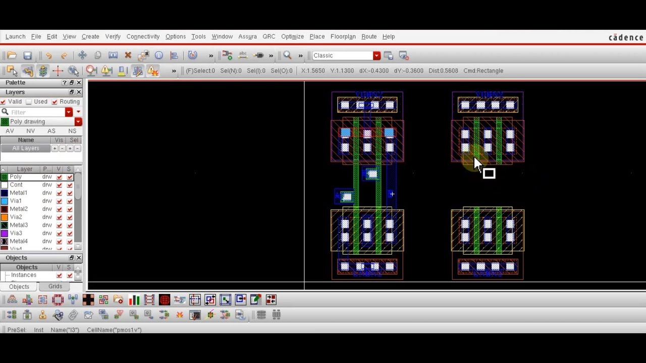
Cadence virtuoso layout from schematic
Cadence virtuoso tutorial: cmos nand gate schematic symbol and layoutNand gate nmos logic transistor schematic using digital universal its ic schematics symbols two given below 1: a 2-input nand gate layout designed in cadence virtuoso.Nand gate circuit and simulation in cadence.
.


